The first transmission electron microscope (TEM) was built by Dr. Ernst Ruska at the University of Berlin in 1931. The need for electron microscopy came from limitations of optical microscopy impossibility of resolving details smaller than the wavelength, about 1 micrometer for the visible light.
Focusing of electron is even easier than that of light just by smartly chosen electrodes and potentials. Electrons can be considered to be waves, the wavelength of an electron accelerated by 10 keV voltage is 0.1 Å (1 Å=
10-10 m). Theoretically, this could be the resolution of electron microscopes; in practice the best achieved is about 1 Å, what allows to see single
atoms.
Modern microscopes are similar to he first one a column of electrodes, focusing electrons on the sample and a detector for reflected (scanning, SEM) or transmitted electrons (TEM, requires very thin samples).
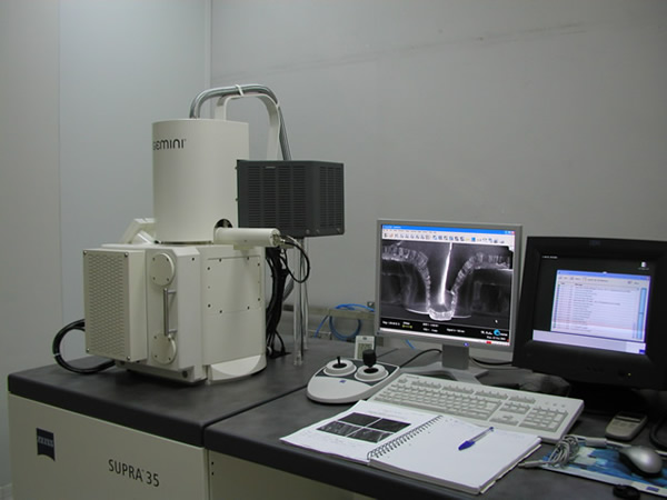
http://www.imm.cnr.it/imm/facilities/images/SEM_FEG_ct.jpg
Caratteristiche: SUPRA 35 High Resolution FESEM (Zeiss)
Caratteristiche: SUPRA 35 High Resolution FESEM (Zeiss)
Sorgente ad emissione di campo tipo Schottky
Tensione di accelerazione da 0,1 kV a 30 kV in modo continuo.
Risoluzione (Con Autolevelling antivibration system): 1.0nm @ 20kV WD = 2mm, 1.7nm @ 15kV WD = 2mm, 1.9nm @ 10kV WD = 2mm, 2.1nm @ 1kV WD = 2mm, 5.0nm @ 0.2kV WD = 2mm
Corrente di fascio: da 4 pA a 10 nA
3 Detector: Detector di SE in-lens, Detector E-T in chamber, Rivelatore di elettroni retrodiffusi
Possibilità di inserimento di fette di diametro fino a 8
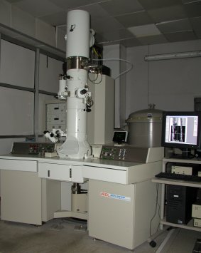
http://www.imm.cnr.it/imm/facilities/images/TEM_FEG_Catania.JPG
Il laboratorio di microscopia di Catania è equipaggiato con due microscopi elettronici in trasmissione. Quello mostrato qui è un JEOL JEM 2010F con sorgente ad emissione di
campo.
La configurazione elettro-ottica dello strumento è da ultra alta risoluzione (risoluzione punto-punto pari a 0.19 nm). Inoltre, il microscopio è equipaggiato con l'apparato GIF (Gatan Image Filter) che consente di realizzare immagini filtrate su finestre strette dello spettro in perdita di energia degli elettroni trasmessi. Questo microscopio è intensamente utilizzato per la caratterizzazione di nanostrutture ed interfaccie laddove è richiesta una elevata sensibilità agli elementi chimici combinata con un'alta risoluzione spaziale.
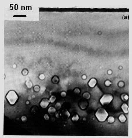
These nice, hexagonal 20 nm bubbles in silicon are caused by implantation of helium ions and successive
anneling.
He-vacancy interactions in Si and their influence on bubble formation and evolution
V. Raineri and S. Coffa, E. Szilágyi, J. Gyulai, E. Rimini
Phys. Rev. B 61, 937945 (2000)
Scanning electron microscopy, even with small magnifications, shows many interesting details, like this complex eyes of an insect. (credits to University of Queensland)
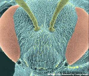
Insect Head (Colour Enhanced) x65Head of an adult insect of the
biting/chewing variety.
Copyright: Nanoworld Image
Gallery
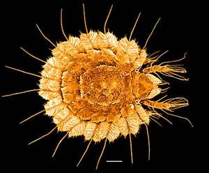
Cepheidae, nymph , Oribatida, Cepheoidea
Copyright: Nanoworld Image
Gallery
One of the common names for oribatid mites is 'beetle mites' because, like many beetles, their legs and bodies are encased in a hard, and often shiny brown armour. However, immature stages of higher oribatid mites usually lack extensive armour plating and look quite different from the adults - so different that associating adults and immatures is one of the challenges of oribatology.
Scale bar = 100 microns.